A node.js-powered 8-bit CPU - part four
This post is part four of a series, the other posts available are
In part two we constructed a circuit using shift registers whereby we could write a byte of data and then read it back in. In part three we booted a 6309 CPU and ran it with a hard-coded operation on the data bus. In this final post, we will put the two together so that we can write arbitrary data onto the data bus and then read back any results.
First, we need to introduce one more 7400-series IC, the 74HC14 hex inverter.
Inverters
These are really simple chips, all they do is take input on a pin, and then output the opposite onto another pin.
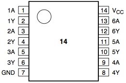
The “A”s are input and “Y”s are output. So, inputting a 0 into 1A/Pin1
results in a 1 being output from 1Y/Pin2. No need for any clocks, just
power, and we have 6 converters available.
Hooking It All Up
Ok, let’s connect everything up. Here’s what we need to do:
-
Connect the two bread boards together, with the shift register board above the CPU board. The bread boards have tongue and groove joints for a snug fit.
-
Wire up +5V and ground rails between the two so that they both have power from a single source.
-
Wire up the D0-D7 data bus from the 6309 to the data bus on the shift register board - it is easiest to hook them in just below the green LEDs.
The GPIO pins from the Raspberry Pi are connected as follows:
-
GPIO17/Pin11 goes to Q on the 6309.
-
GPIO18/Pin12 goes to E on the 6309.
-
GPIO21/Pin13 goes to STCP on the 74HC595.
-
GPIO22/Pin15 goes to DS on the 74HC595.
-
GPIO23/Pin16 goes to Q7 on the 74HC165.
-
GPIO24/Pin18 goes to RESET on the 6309.
There are 4 more connections we need to make, which is where the 74HC14 comes in.
RW On The 6309
The RW pin on the 6309 denotes whether from the 6309’s point of view the bus is being written to or read from. When high, the 6309 is reading, and when low, it is writing.
We can use this feature to automatically switch the OE (“output enable”) pin on the 74HC595 on or off, so that when the 6309 is reading OE is enabled, and when it is writing OE is disabled, leaving the data bus clear for the 6309s data. In this way the bus can be shared between devices.
However, we cannot connect them directly, as the logic is the wrong way around
- we want OE to be low when RW is high and vice versa. So, we use the 74HC14, and by connecting them through pins 1A and 1Y on the 74HC14, we get the logic we want.
PL On The 74HC165
The final connection we need to make is a way to trigger the 74HC165 to read from the data bus, so that we can get data back into the Raspberry Pi.
The solution for this is to wire the 74HC165’s PL pin to clock E on the 6309. This isn’t immediately obvious, but is determined by careful reading of the 6309’s datasheet. The quality of the image below isn’t great, but it shows when data from the 6309 is valid.
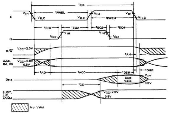
The part we are interested in is the “Data” line, and the timing when the data is readable is the time between the Q clock going low and the E clock going low.
So, for my design, I have hooked up the PL pin to the inverse (again, going through the 74HC14 to invert the logic) of the Q clock, using pins 2A and 2Y. This way, whenever Q goes low, the 74HC165 reads whatever is on the data bus at that time, and if this happens to be at a point when we want to grab data from the 6309, it should be valid at that point in time and we then just need to shift the data out of the 74HC165 before the next Q clock when the data will be replaced.
The finished boards should look something like this:
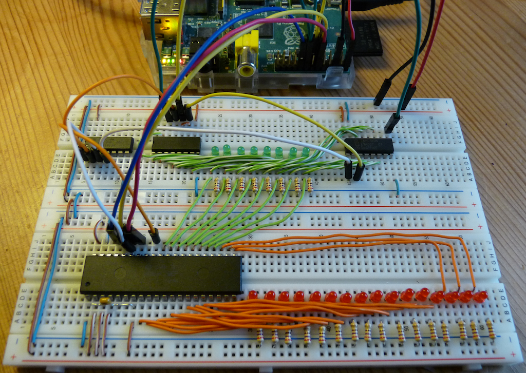
The 74HC14 is at the top left, with the orange and white jumper wires used for the inverted connections.
Software
At this point we are done with the hardware, and can move to software. First we need to come up with a program, and for this I have chosen a very simple one
- add two numbers together and return the result. The code is below.
;
; Add two 16-bit numbers (doubles) together.  The final version will accept
; arbitrary numbers on the command line, but for now we hard code two numbers
; which helps us to understand the opcodes.
;
	LDD	#$04	; Load 4 into the D register (D=4)
	ADDD	#$05	; Add 5 to D and save the result (D=D+5)
	STD	$B6B7	; Store the value of D to address 0xB6B7
By using asm6809.pl and od we can look at what the instruction opcodes need
to be.
$ asm6809.pl -o 6309-adder 6309-adder.s

$ od -t x1 6309-adder
0000000    cc  00  04  c3  00  05  fd  b6  b7
0000011
From this we can determine:
-
0xccis the opcode forLDDwith an immediate value. -
0xc3is the opcode forADDDwith an immediate value. -
0xfdis the opcode forSTDto store at an extended address.
An immediate value is one that is used as-is for the data, rather than being an address containing the data. An extended address is where a full address is specified, rather than an offset. Different addressing modes result in different opcodes, as the instruction needs to do different things.
Now that we have our opcodes, we need to find out how many cycles each of them take to complete. As we are hard coding every clock cycle in this set up, it is critical that we read and write data at exactly the right time. The best reference I’ve found for the 6809/6309 is here and it gives the number of bytes and clock cycles for every instruction.
At this point we have all the information required, and it is a Simple Matter Of Programming. My script to add two arbitrary numbers using the 6309 going via the shift registers for input and output is below. The comments inline hopefully explain exactly what is happening.
var rpio = require('rpio');

/*
 * The two numbers to add together from command line arguments.
 */
var num1 = parseInt(process.argv[2], 10);
var num2 = parseInt(process.argv[3], 10);

/*
 * Set up our pin mappings and configure them.
 */
var pin = {
	'clockQ': 11,
	'clockE': 12,
	'clockS': 13,
	'write': 15,
	'read': 16,
	'reset': 18,
}

rpio.setOutput(pin.clockQ);
rpio.setOutput(pin.clockE);
rpio.setOutput(pin.clockS);
rpio.setOutput(pin.write);
rpio.setInput(pin.read);
rpio.setOutput(pin.reset);

// Start everything low.
rpio.write(pin.clockQ, 0);
rpio.write(pin.clockE, 0);
rpio.write(pin.clockS, 0);
rpio.write(pin.write, 0);
rpio.write(pin.reset, 0);

/*
 * Clocks - 'sixclock' for the 6309, 'shiftclock' for the shift registers.
 */
var sixclock = function ()
{
	rpio.write(pin.clockQ, 1);
	rpio.write(pin.clockE, 1);
	rpio.write(pin.clockQ, 0);
	rpio.write(pin.clockE, 0);
}
var shiftclock = function ()
{
	rpio.write(pin.clockS, 1);
	rpio.write(pin.clockS, 0);
}

/*
 * Shift a byte of data out to the 74HC595.
 */
var shiftout = function (data)
{
	// Convert the hex to a binary string
	var bits = String("00000000" + data.toString(2)).slice(-8);

	bits.split('').forEach(function (bit) {
		rpio.write(pin.write, bit);
		shiftclock();
	});
	shiftclock();
}

/*
 * Shift a byte of data in from the 74HC165, returning as a hex value.
 */
var shiftin = function ()
{
	var inbyte = "";
	for (var i = 0; i < 8; i++) {
		inbyte += rpio.read(pin.read);
		shiftclock();
	}
	return String("00" + parseInt(inbyte, 2).toString(16)).slice(-2);
}

/*
 * Convert a 16-bit number to an array of two 8-bit hexadecimals.
 */
var dec2hex16 = function (number)
{
	var num = String("0000" + number.toString(16)).slice(-4);

	return [parseInt(num.slice(0,2), 16), parseInt(num.slice(2,4), 16)];
}

/*
 * Initialise the 6309, starting with 10 cycles with the RESET line held down
 * to clear all state.  We then run for 3 cycles after RESET - one to load in
 * the RESET, and two to get the chip ready.
 *
 * The number of cycles required here was determined by experimentation.
 */
for (var i = 0; i < 10; i++) {
	sixclock();
}
rpio.write(pin.reset, 1);
for (var i = 0; i < 3; i++) {
	sixclock();
}

/*
 * At this point we are ready to read in the first address.  The 6309's RESET
 * vector is at $FFFE-$FFFF, which is the hardcoded location where it reads
 * the first address from.
 *
 * We provide the starting address of $1020, though it is somewhat arbitrary,
 * and we could use any address except for $FFF0-$FFFF which is reserved.
 */
shiftout(0x10); sixclock();	// Load address from $FFFE
shiftout(0x20); sixclock();	// Load address from $FFFF

/*
 * Jump to the first address (0x1020) that we input.  After that we can
 * start to input our first instruction.
 */
sixclock();

/*
 * LDD our first number.
 */
var lddbytes = dec2hex16(num1);
shiftout(0xcc); sixclock();		// LDD immediate
shiftout(lddbytes[0]); sixclock();	// Read in num1's high byte
shiftout(lddbytes[1]); sixclock();	// Read in num1's low byte

/*
 * ADDD our second number.  ADDD with an immediate is a 4 cycle
 * instruction so we have an additional clock at the end.
 */
var adddbytes = dec2hex16(num2);
shiftout(0xc3); sixclock();		// ADDD immediate
shiftout(adddbytes[0]); sixclock();	// Read in num2's high byte
shiftout(adddbytes[1]); sixclock();	// Read in num2's low byte
sixclock();				// Clock to perform ADDD operation

/*
 * STD the result to an arbitrary memory location, in this case we have
 * chosen address $C880 but it is irrelevant as we ignore it.
 *
 * STD extended is a 6 clock instruction, with the two byte result available
 * on the data bus during cycles 5 and 6.
 */
shiftout(0xfd); sixclock();		// STD extended
shiftout(0xc8); sixclock();		// Read in $C8 high byte
shiftout(0x80); sixclock();		// Read in $80 low byte
sixclock();				// Clock operation
sixclock(); byte1 = shiftin();		// Write high byte to memory
sixclock(); byte2 = shiftin();		// Write low byte to memory

/*
 * We are done, output the calculation.
 */
console.log("%d + %d = %d", num1, num2, parseInt("0x" + byte1 + byte2, 16));

/*
 * Reset the CPU to be nice, and to clear the LEDs.  Four clocks appear to be
 * enough to complete the reset.
 */
rpio.write(pin.reset, 0);
for (var i = 0; i < 4; i++) {
	sixclock();
}
We can run the program as follows.
# node 6309-adder.js 1 2
1 + 2 = 3
The output appears to be the correct answer. We now have a fully functioning co-processor attached to our Raspberry Pi ;)
Of course, there are some limitations. As we are dealing with 16-bit numbers, we can overflow:
# node 6309-adder.js 32768 32767
32768 + 32767 = 65535
# node 6309-adder.js 32768 32768
32768 + 32768 = 0
However, adding support for that and executing arbitrary instructions is left as an exercise for the reader!
Hopefully this was interesting. It has certainly been very useful for me to learn exactly what is going on at the hardware level, and I’d strongly encourage anyone involved in software development to do likewise - it gives you a new appreciation for the operations involved in running your code.
All Posts
- 16 Jul 2015 » Reducing RAM usage in pkgin
- 03 Mar 2015 » pkgsrc-2014Q4: LTS, signed packages, and more
- 06 Oct 2014 » Building packages at scale
- 04 Dec 2013 » A node.js-powered 8-bit CPU - part four
- 03 Dec 2013 » A node.js-powered 8-bit CPU - part three
- 02 Dec 2013 » A node.js-powered 8-bit CPU - part two
- 01 Dec 2013 » A node.js-powered 8-bit CPU - part one
- 21 Nov 2013 » MDB support for Go
- 30 Jul 2013 » What's new in pkgsrc-2013Q2
- 24 Jul 2013 » Distributed chrooted pkgsrc bulk builds
- 07 Jun 2013 » pkgsrc on SmartOS - creating new packages
- 15 Apr 2013 » What's new in pkgsrc-2013Q1
- 19 Mar 2013 » Installing SVR4 packages on SmartOS
- 27 Feb 2013 » SmartOS is Not GNU/Linux
- 18 Feb 2013 » SmartOS development preview dataset
- 17 Jan 2013 » pkgsrc on SmartOS - fixing broken builds
- 15 Jan 2013 » pkgsrc on SmartOS - zone creation and basic builds
- 10 Jan 2013 » Multi-architecture package support in SmartOS
- 09 Jan 2013 » Solaris portability - cfmakeraw()
- 08 Jan 2013 » Solaris portability - flock()
- 06 Jan 2013 » pkgsrc-2012Q4 illumos packages now available
- 23 Nov 2012 » SmartOS and the global zone
- 24 Oct 2012 » Setting up Samba on SmartOS
- 10 Oct 2012 » pkgsrc-2012Q3 packages for illumos
- 23 Aug 2012 » Creating local SmartOS packages
- 10 Jul 2012 » 7,000 binary packages for OSX Lion
- 09 Jul 2012 » 9,000 packages for SmartOS and illumos
- 07 May 2012 » Goodbye Oracle, Hello Joyent!
- 13 Apr 2012 » SmartOS global zone tweaks
- 12 Apr 2012 » Automated VirtualBox SmartOS installs
- 30 Mar 2012 » iptables script for Debian / Ubuntu
- 20 Feb 2012 » New site design
- 11 Jan 2012 » Set up anonymous FTP upload on Oracle Linux
- 09 Jan 2012 » Kickstart Oracle Linux in VirtualBox
- 09 Jan 2012 » Kickstart Oracle Linux from Ubuntu
- 22 Dec 2011 » Last day at MySQL
- 15 Dec 2011 » Installing OpenBSD with softraid
- 21 Sep 2011 » Create VirtualBox VM from the command line
- 14 Sep 2011 » Creating chroots for fun and MySQL testing
- 30 Jun 2011 » Graphing memory usage during an MTR run
- 29 Jun 2011 » Fix input box keybindings in Firefox
- 24 Jun 2011 » How to lose weight
- 23 Jun 2011 » How to fix stdio buffering
- 13 Jun 2011 » Serving multiple DNS search domains in IOS DHCP
- 13 Jun 2011 » Fix Firefox URL double click behaviour
- 20 Apr 2011 » SSH via HTTP proxy in OSX
- 09 Nov 2010 » How to build MySQL releases
- 29 Apr 2010 » 'apt-get' and 5,000 packages for Solaris10/x86
- 16 Sep 2009 » ZFS and NFS vs OSX
- 12 Sep 2009 » pkgsrc on Solaris
- 09 Dec 2008 » Jumpstart from OSX
- 31 Dec 2007 » Set up local caching DNS server on OSX 10.4